CMOS SWIR+
Reimagine new wide-spectrum imaging

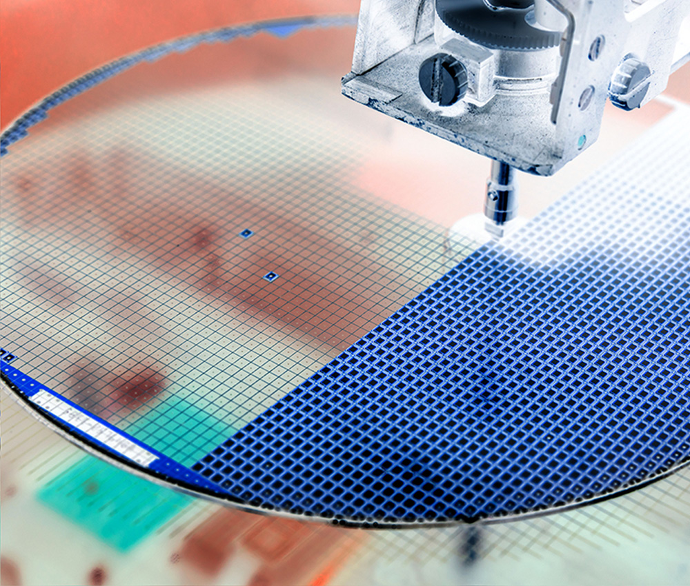
Turning scientific innovation into commercial applications, Aritlux has developed the world’s first single-chip GeSi CMOS-based and dual-mode (2D/3D) SWIR sensing technology at TSMC on 12-inch production line, and is ready for commercialization at scale.
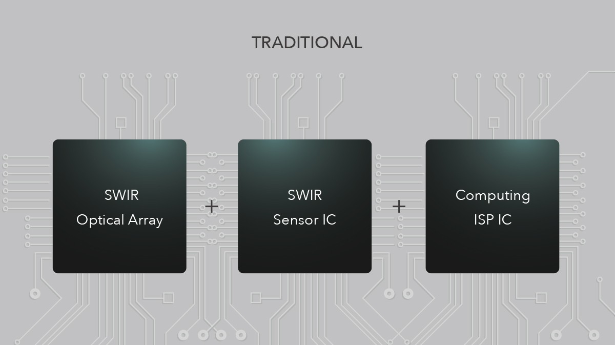
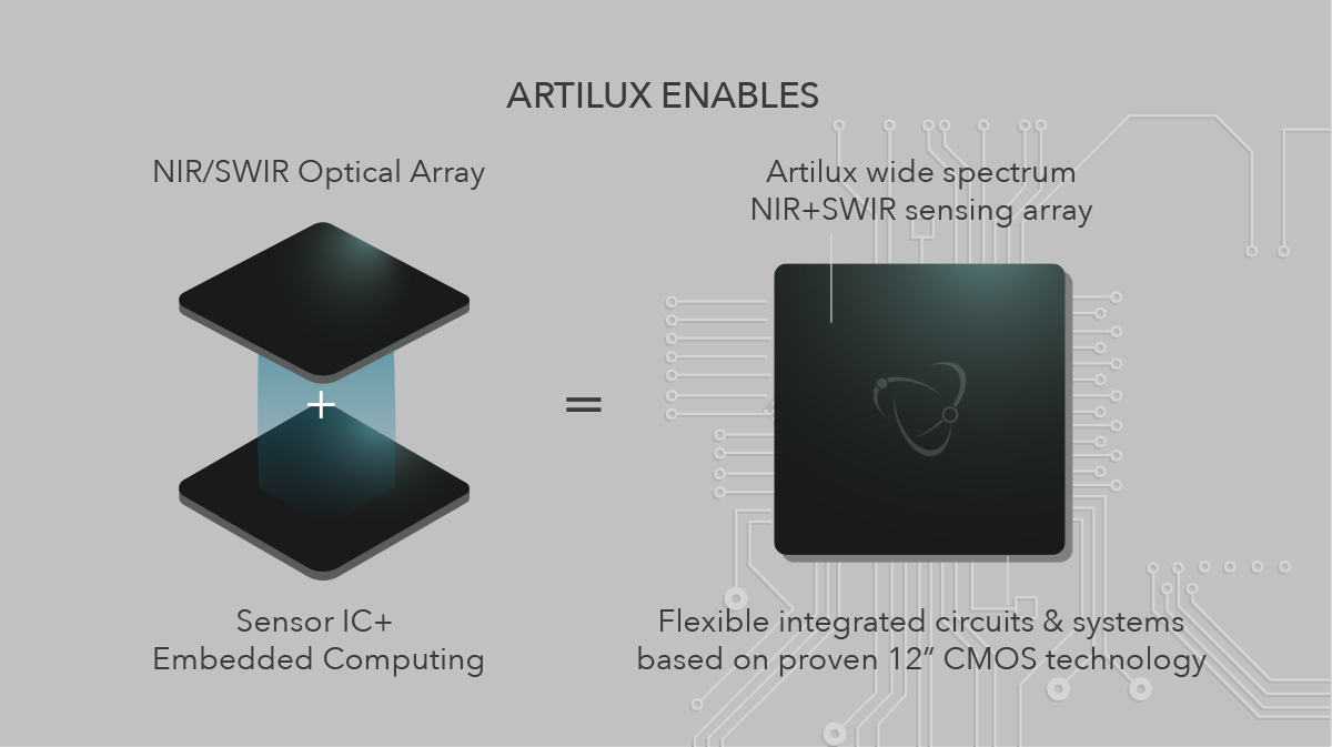
Today, SWIR sensing is mostly based on GaAs or InP substrates and other III-V compound semiconductor, resulting in high cost especially with growing demand for larger array size, and growing difficulty to be integrated with CMOS-based circuity. With our proprietary and patented GeSi technology for SWIR 2D, 3D imaging and beyond, Artilux enables an ever-growing ecosystem to meet the market needs for a compact, ultra-sensitive, low power consumption, safe (lead-free), cost-competitiveness and mature SWIR all-in-one sensor.
The Infrared (IR) spectrum is placed between the visible and microwave regions, which spans from 0.75 to 12 micron (μm), and can be classified into 4 sub-bands: Near Infrared (NIR), Short Wave Infrared (SWIR), Mid Wave Infrared (MWIR), and Long Wave Infrared (LWIR).

High accuracy and high resolution in different environments under low visibility (e.g., imaging in fog, imaging at night), unique recognition capability on specific object materials (e.g., plastics, stones, glass, etc.)
12 inch-foundry production, diversified product designs to meet a variety of needs
Single chip with integrated edge AI computing capability in a compact, low power, and multi-functional design
Low risk to human eyes from laser exposure, less interference from sunlight and ambient noise
Significant cost-saving of sensor over conventional III-V technology